Courses & Events
The Past, Present, and Future of Technology Innovation in Japan
Wednesday, Feb 17, 2016
04:15 pm - 05:30 pm
The Past, Present, and Future of Technology Innovation in Japan: A View From the Front Lines of Semiconductor Process
Tool Development
In this presentation, Dr. Suzuki describes the complex dynamics that have governed semiconductor technology development in Japan, including the interplay between technology pull (strategic application demands from domains that range from aerospace to consumer products) and technology push (as exemplified by Moore’s Law and ITRS roadmapping). Dr. Suzuki will also comment on current technology management challenges for continuing innovation in the ecosystem around semiconductor IC technologies and on future prospects for Japan’s contributions to this area.
A graduate of the University of Tokyo, Dr. Suzuki joined Canon in 1973, where he was engaged in developing a wide range of lithography tools for semiconductor fabrication, including aligners (contact/proximity, mirror projection), steppers (g-line, i-line, and KrF), scanners (KrF, ArF, F2, and immersion), EUV systems, and nano-imprint lithography. Since 1984, he was responsible for the optics of Canon exposure tools. In 2014, he left Canon, and joined Gigaphoton as a technical advisor.
Dr. Suzuki’s work covers all of the optics areas of lithography: projection optics (mirror projection optics, stepper/scanner lenses, and intelligent control of the projection system), illumination system, alignment/focusing optics and metrology. In particular, he developed various resolution enhancement technologies, such as quadrupole illumination and double exposure method in 1D. Dr. Suzuki became a Canon Fellow in 2004, and he was elected as an SPIE Fellow in 2005. He is the first-ever SPIE Fellow from Japan in the lithography field. In 2015, he joined the Board of Directors of SPIE. Dr. Suzuki has published more than 50 papers about microlithography, and he has obtained 138 Japanese patents and 111 patents in the United States.
***
This session is presented by the US-Asia Technology Management Center.
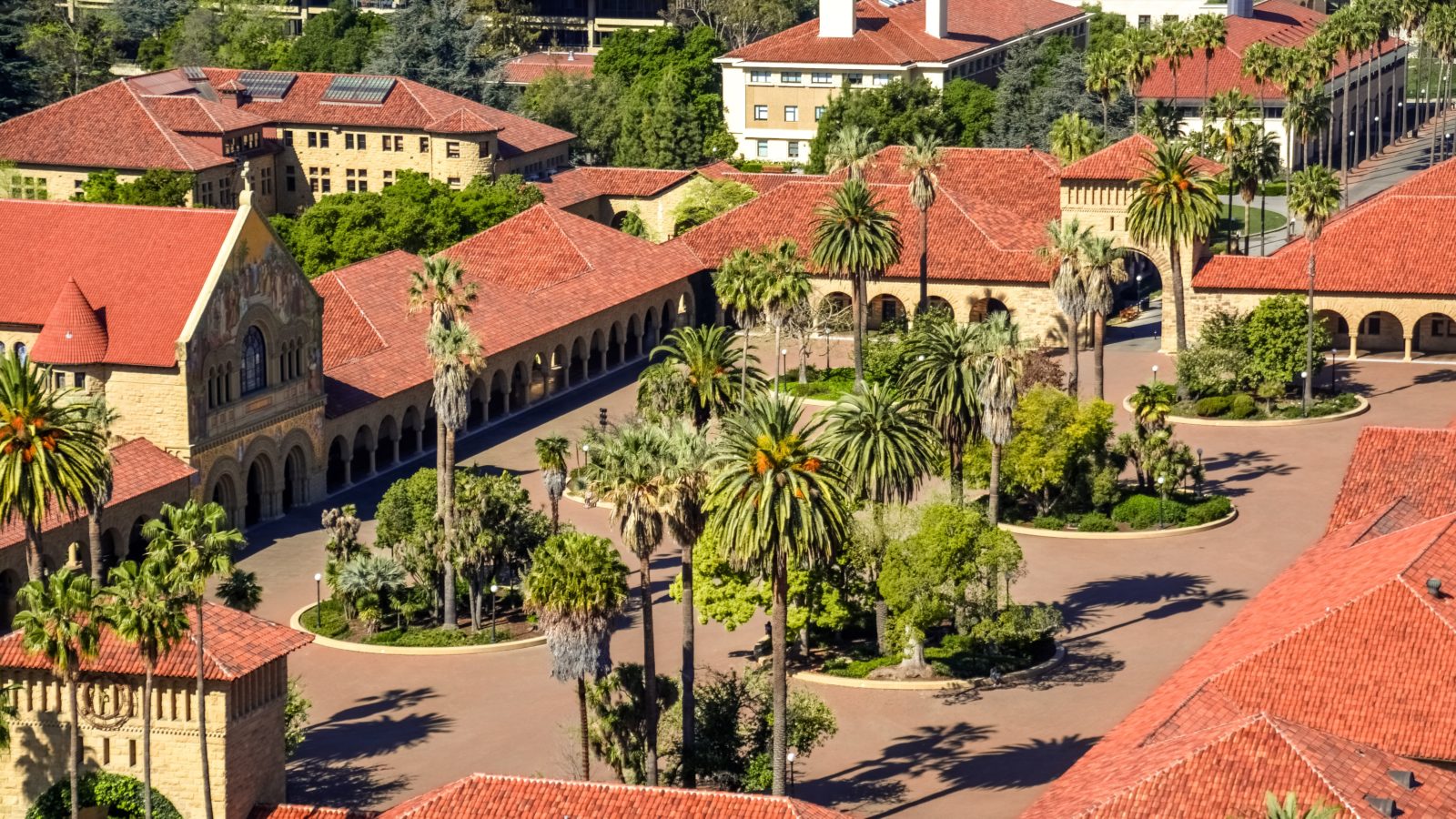
Stanford University | CISX Auditorium 420 Via Palou Mall • Stanford, CA Wednesday, February 17, 2016 • 4:30-6:00PM
